


Published on Nov 30, 2023
Fourth generation wireless and mobile system are currently the focus of research and development. Broadband wireless system based on orthogonal frequency division multiplexing will allow packet based high data rate communication suitable for video transmission and mobile internet application. Considering this fact we proposed a data path architecture using dedicated hardwire for the baseband processor.
The most computationally intensive part of such a high data rate system are the 64-point inverse FFT in the transmit direction and the viterbi decoder in the receiver direction. Accordingly an appropriate design methodology for constructing them has to be chosen a) how much silicon area is needed b) how easily the particular architecture can be made flat for implementation in VLSI c) in actual implementation how many wire crossings and how many long wires carrying signals to remote parts of the design are necessary d) how small the power consumption can be. This paper describes a novel 64-point FFT/IFFT processor which has been developed as part of a large research project to develop a single chip wireless modem.
The complete structure of a modern specified by the IEEE 802.11a standard is shown in fig. 1. It consists of a data scrambler, modulator, convolutional encoder, interleaver, 64-point IFFT/FFF, demodulator, deinterleaver, Viterbi decoder, and descrambler. The standard specifies a data rate ranging from 6 to 54 Mb/s. Depending on the de d rate, the modulation scheme adopted can be binary phase shift keying (BPSKt, quaternary phase shift keying (QPSK), or quadrature amplitude modulation(QAM) with l-6bit/subcarrier.
The encoding rates supported in the standard are 1/2, 2/3, and 3/4. The bandwidth of the transmitted signal is 20 MHz and the OFDM symbol duration is 4 ?s including 0.8 ?s for a guard interval [1 ] Thus, in effect, FFT/TFFT has to be computed within 4 ?
In general, the FFT implementations typically fall into one of the two categories: 1) methods based on direct Fourier transform [and 2) methods based on direct hardware implementations of established FFT signal flow graphs [8] [14]. A problem with these solutions is that the approach adopted on the algorithmic level typically takes little account of its implications at the architecture, data flow, or chip design levels. Thus, many of these designs [8]-[10] may be irregular, dominated by wiring, and may have heavy overheads in terms of data storage [15] In a complex system, deployment of such strategies may result in severe disadvantages, because of the tight timing constraints and implicit requirement of low power consumption.
The conventional Cooley-Tukey radix-2 FFT algorithm requires 192 complex butterfly operations for a 64-point FFT computation. Considering that one FF1' has to be computed within 4?s, one butterfly operation has to be completed within 20,8 ns which results in 48 MHz clock frequency for a single butterfly architecture. The synthesis result for a radix-2 butterfly unit (one complex multiplication and two complex additions) in 1HP O.25?m- technology shows that it occupies 0.18-mm area and dissipates 17 mW power at that frequency.
On top of this butterfly unit, one needs memory to store the complex twiddle factors and complex intermediate data, serial-to-parallel and parallel-to-serial converters at the inputs and outputs, respectively, complicated addressing logic and control circuitry. Combining all these circuit modules it is expected that the power dissipation of the entire processor will be quite high. Moreover, the input data arrives at 20 MHz clock frequency, and thus, it is more appropriate to operate the FFT module at that frequency.
In order to satisfy the time constraint at this frequency, one has to employ multiple butterfly units in parallel, which in turn increases the area and power dissipation. Alternatively, since most of the implementations of the IEEE 802.1 1a standard oversample the incoming data at 40 or 80 MHz, a single radix-2 butterfly based FFT module should be operated at 80 MHz clock frequency (the next available frequency to the actually required frequency). This approach satisfies the timing constraint, but at the cost of high power consumption.
In order to speed up the FFT computation, more advanced solutions have been proposed using an increase of the radix [15] [16]. These approaches result in increase of arithmetic complexity within the butterfly itself. The radix-4 FFT algorithm is most popular and has the potential to satisfy the current need. However, a single radix-4 butterfly requires three complex multiplications and eight complex additions. Thus, in order to carry out one radix-4 butterfly operation per clock cycle, one needs to complete 12 real multiplications and 16 real additions at each cycle. Since multipliers are typically very power-hungry elements in a VLSI design, this type of arrangement results in significant power consumption.
The block diagram of 64-point FFT /IFFT processor consist of in put unit ,two 8-point FFT unit, a multiplier unit,an internal storage register bank,an output unit and a 5-bit binary counter
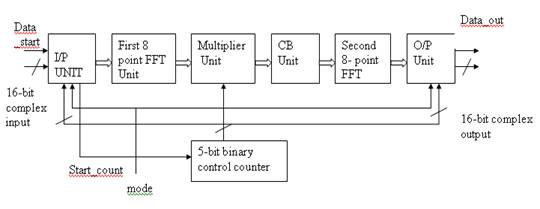
It consists of an input register bank having 16-bit word length that can store 57 complex data .Three additional 16-bit complex storage registers reg1, reg2 and reg 3 are also provided for temporary storage of data.I/P unit is equipped with two single bit signals, MODE and DATA-START. The assertion of data-start signal indicates the presence of serial valid data stream at the input of the register bank and it starts its operation. The data_start signal remains at logic 1 for next 64 cycles. The logic 1 state of the mode signal indicates the IFFT mode of operation, whereas its logic 0 state indicates the FFT mode. when the mode signal is asserted to logic 1 state ,the real and imaginary parts of the incoming serial data stream are swapped before the data are serially inputted to the register bank. On the other hand if the mode signal is at a logic 0 state the real and imaginary parts of the incoming serial data stream are inputted to the register bank without swapping.
To construct the 8 point FFT unit we chose the radix 2 DIT 8 point fft algorithm. In this case we predominantly choose butterfly computations. We exploited this fact and implemented a fully parallel 8 point FFT by exactly following the flow graph of fig 2 using only addition /subtraction and shift and add operation. The internal word length of these units is 16-bit. The computation of an 8-point FFT is carried out in a single clock cycle.
49 non-trivial inter dimensional constants are to be multiplied to the intermediate results coming out from the first 8-point FFT unit. These constants reveals that only nine sets of them are unique, where in each set the first entry corresponds to the cosine function and the second one corresponds to sine function .The entire interdimensional constant multiplication operation can be carried out using only these nine sets of constants. The first set of these constants is trivial. Thus, there are eight set of non-trivial constants required for carrying out the interdimensional constant multiplication operation. The implication is that one requires storage for only these eight sets of constants instead of 49. Thus compared to the conventional DIT FFT algorithm, significantly less storage space in this scheme is needed.
| Are you interested in this topic.Then mail to us immediately to get the full report.
email :- contactv2@gmail.com |
